


Quantum computing is a devilishly complex technology, with quite a few technical hurdles impacting its development. Of these problems two vital problems stand out: miniaturization and qubit good quality.
IBM has adopted the superconducting qubit road map of reaching a 1,121-qubit processor by 2023, foremost to the expectation that 1,000 qubits with today’s qubit type variable is feasible. On the other hand, present-day ways will need quite big chips (50 millimeters on a side, or greater) at the scale of compact wafers, or the use of chiplets on multichip modules. Even though this solution will get the job done, the goal is to attain a greater route towards scalability.
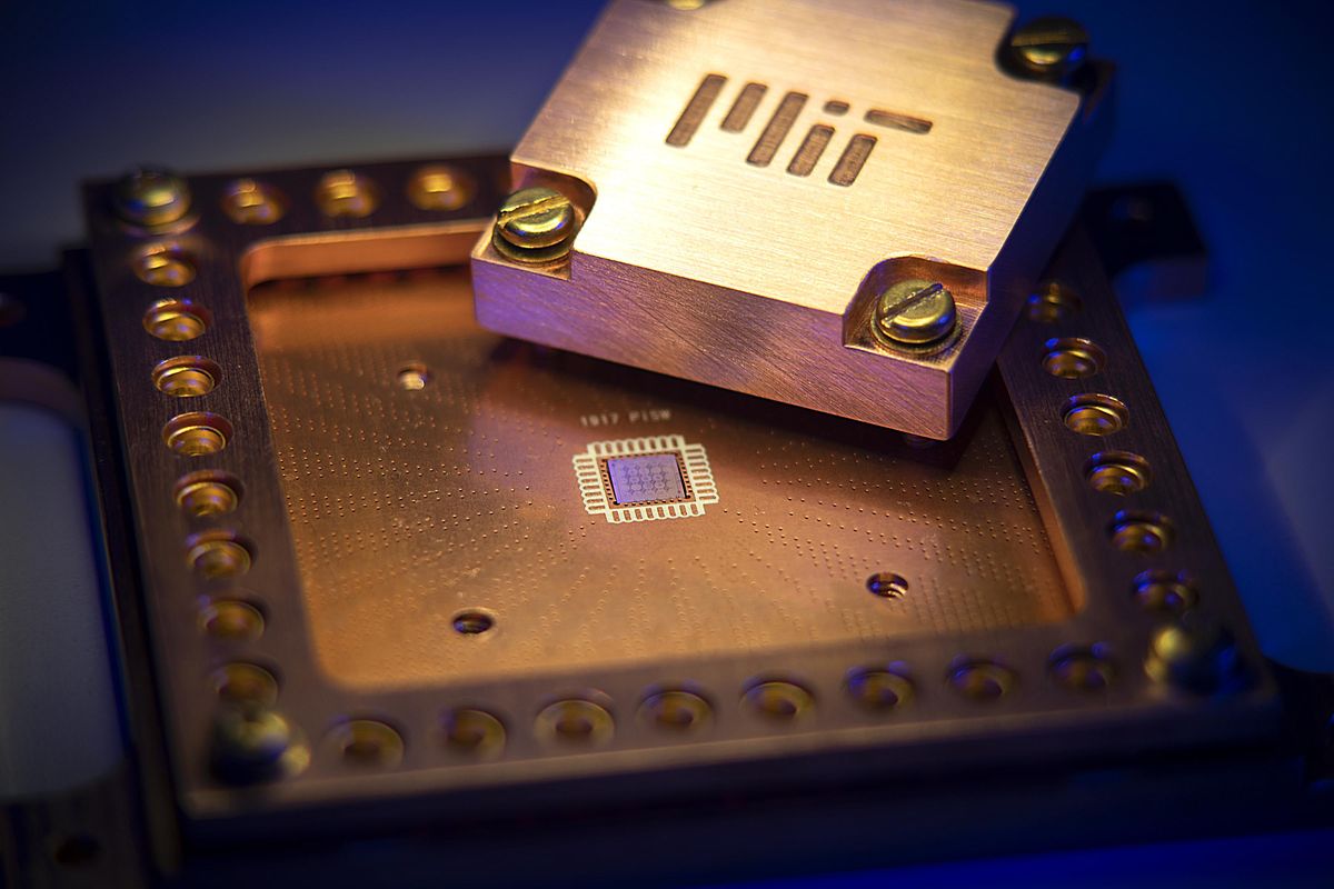
Now scientists at MIT have been ready to both lower the size of the qubits and carried out so in a way that reduces the interference that happens in between neighboring qubits. The MIT researchers have improved the selection of superconducting qubits that can be extra on to a system by a element of 100.
“We are addressing the two qubit miniaturization and top quality,” stated William Oliver, the director for the Center for Quantum Engineering at MIT. “Unlike conventional transistor scaling, wherever only the quantity seriously issues, for qubits, big numbers are not enough, they should also be high-efficiency. Sacrificing general performance for qubit amount is not a useful trade in quantum computing. They need to go hand in hand.”
The crucial to this huge maximize in qubit density and reduction of interference comes down to the use of two-dimensional components, in specific the 2D insulator hexagonal boron nitride (hBN). The MIT researchers demonstrated that a number of atomic monolayers of hBN can be stacked to type the insulator in the capacitors of a superconducting qubit.
Just like other capacitors, the capacitors in these superconducting circuits acquire the variety of a sandwich in which an insulator product is sandwiched involving two metal plates. The large variance for these capacitors is that the superconducting circuits can function only at extremely small temperatures—less than .02 degrees over complete zero (-273.15 °C).
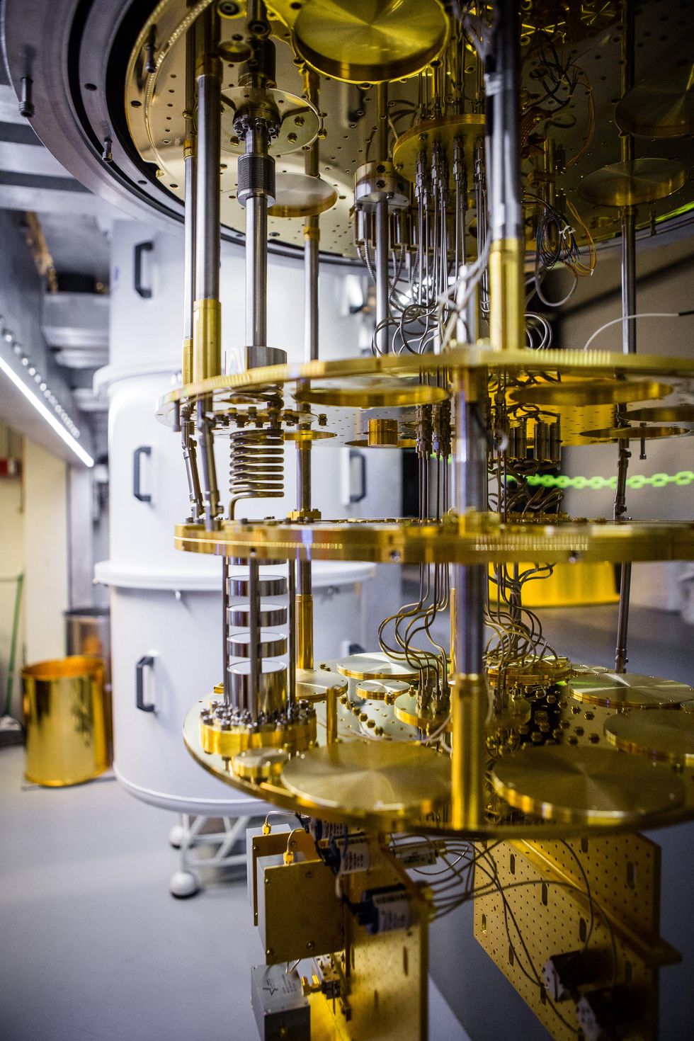
Superconducting qubits are measured at temperatures as lower as 20 millikelvin in a dilution refrigerator.Nathan Fiske/MIT
In that ecosystem, insulating resources that are accessible for the career, these types of as PE-CVD silicon oxide or silicon nitride, have rather a handful of flaws that are also lossy for quantum computing apps. To get all around these materials shortcomings, most superconducting circuits use what are termed coplanar capacitors. In these capacitors, the plates are positioned laterally to one particular a further, fairly than on leading of one one more.
As a end result, the intrinsic silicon substrate underneath the plates and to a smaller diploma the vacuum earlier mentioned the plates serve as the capacitor dielectric. Intrinsic silicon is chemically pure and hence has number of defects, and the significant measurement dilutes the electric powered industry at the plate interfaces, all of which qualified prospects to a low-loss capacitor. The lateral size of every single plate in this open up-confront style ends up becoming fairly large (typically 100 by 100 micrometers) in purchase to attain the essential capacitance.
In an work to shift away from the substantial lateral configuration, the MIT scientists embarked on a search for an insulator that has pretty couple defects and is appropriate with superconducting capacitor plates.
“We chose to review hBN mainly because it is the most widely employed insulator in 2D content research thanks to its cleanliness and chemical inertness,” explained colead writer Joel Wang, a investigate scientist in the Engineering Quantum Techniques group of the MIT Research Laboratory for Electronics.
On either side of the hBN, the MIT researchers made use of the 2D superconducting material, niobium diselenide. One particular of the trickiest elements of fabricating the capacitors was operating with the niobium diselenide, which oxidizes in seconds when exposed to air, in accordance to Wang. This necessitates that the assembly of the capacitor happen in a glove box crammed with argon fuel.
While this would seemingly complicate the scaling up of the output of these capacitors, Wang does not regard this as a limiting factor.
“What establishes the high quality component of the capacitor are the two interfaces amongst the two materials,” said Wang. “Once the sandwich is produced, the two interfaces are “sealed” and we really don’t see any obvious degradation over time when uncovered to the environment.”
This absence of degradation is since close to 90 % of the electrical discipline is contained inside the sandwich composition, so the oxidation of the outer floor of the niobium diselenide does not participate in a important job anymore. This finally can make the capacitor footprint a great deal more compact, and it accounts for the reduction in cross speak involving the neighboring qubits.
“The primary obstacle for scaling up the fabrication will be the wafer-scale expansion of hBN and 2D superconductors like [niobium diselenide], and how just one can do wafer-scale stacking of these films,” included Wang.
Wang thinks that this study has revealed 2D hBN to be a very good insulator prospect for superconducting qubits. He states that the groundwork the MIT workforce has completed will provide as a highway map for working with other hybrid 2D supplies to make superconducting circuits.
More Stories
Unlocking Startup Potential: Why Employee Monitoring Software is a Game-Changer in 2025
Ossisto Powers Your Growth with Smart Outsourcing
How a SaaS Marketing Agency Can Help Your Software Business Grow